
ASSIGMENT - redraw the echo hello-world board, add (at least) a button and LED (with current-limiting resistor) check the design rules, and make it
Unfortunately I was unable to complete the weeks assignment as we have not yet received our materials and components. This week will be available as soon as possible.
HELLO ECHO {UPDATE}
Downloaded and installed eagle.
As we are still awasiting our crystals and resonators we did research on using the internal clock of the ATtiny44 (which runs at 8Mhz but not as constantly as an external oscillator) and with guidance from Ohad, our GURU we will do a group project to see if and how it works without the resonator.
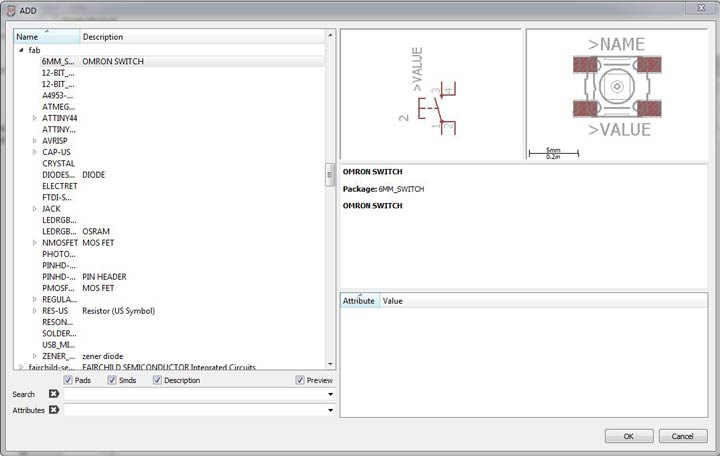
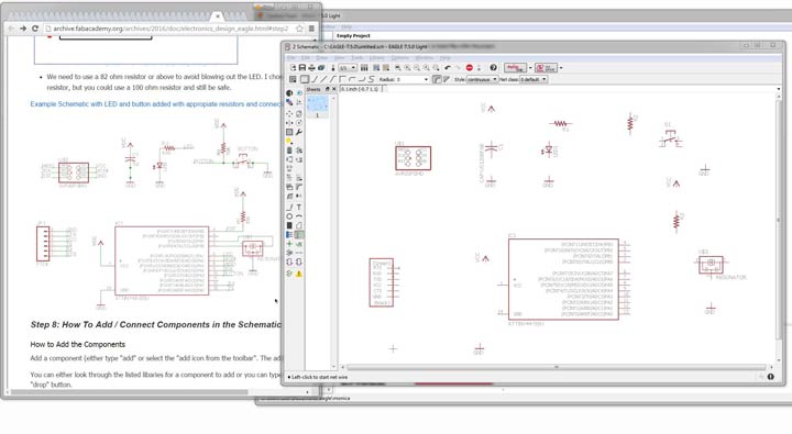
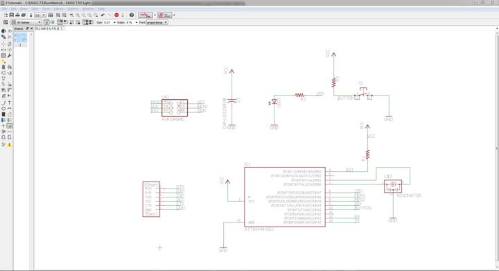
After reading many tutorials (SPARKFUN-electronics, SPARKFUN-schematic, SPARKFUN-board layout, FABACADEMY-intro to eagle, FABACADEMY-custom outlines) and learning about the components, I started the schematic, I used the single LED schematic as reference.
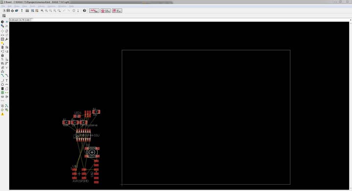
I started by choosing components from the libraries installed (fab.lbr and adafruit.lbr) and laying them out according to the refernce schematic
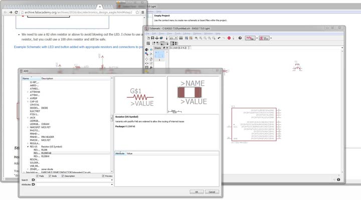
This didn't go to badly, once you understood the way that eagle works
right click rotates the part
Grouping you have to group the selected items to move them as a whole, whilst holding down control and moving it with the right mouse held down.
Net tomake logical connections between components, if this is not done correctly you will not have the connection on the board to route correctly, you can however switch back to the schematic and relink or fix this , which then automatically updates the board when switching back.
Junction to add the big round green dots.
Label to name display components.
I then went to file>switch to board
It was only at this stage that I realised that the layout in the schematic is not quite as important, as it gets jumbled up again in the board layout.
Moving all the pieces onto the board went fine as well, but when rats nested and auto routed it just came out a jumble every time.
At first I thought it was normal but decided to read up on it and discovered that there should not be yellow connector lines left over, and also not blue lines indicating a double layered board, which we are not using.
I tried setting the auto run to only use the top layer, but that still left me with unconnected yellow lines.
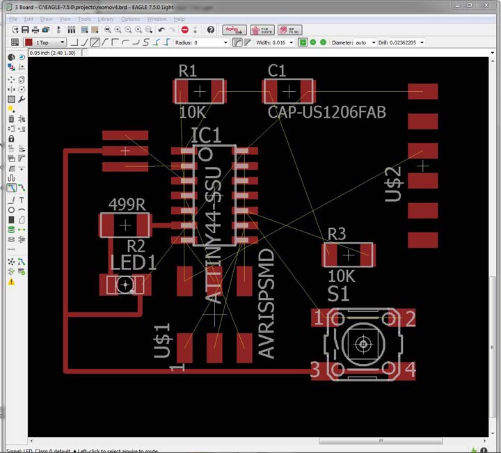
It was at this point that I went back to the fabacademy tutorial about connecting the components manually, also that they need to be rotated further to get best results. Once I had all the compnents linked I used the different line tools to make the lines more interesting.
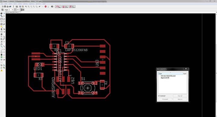
On the bottom layer I drew out my outline shape.
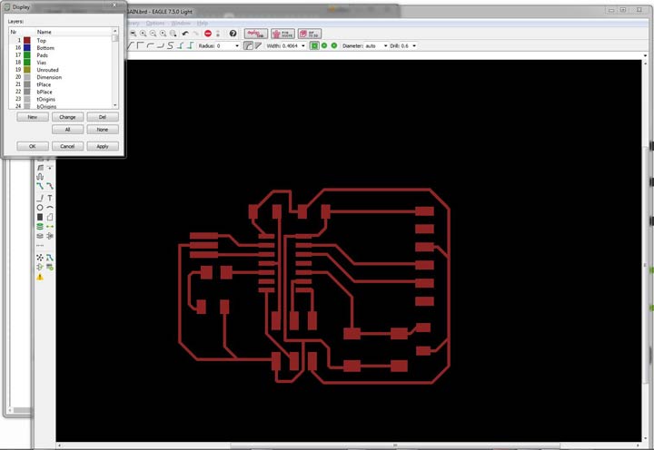
I activated only the top layer and exported the it , file>export>image to png, I then activated (unactivating the top layer) to export separately for the cut out shape.
Settings for export were monochrome, 500dpi, full image, .png
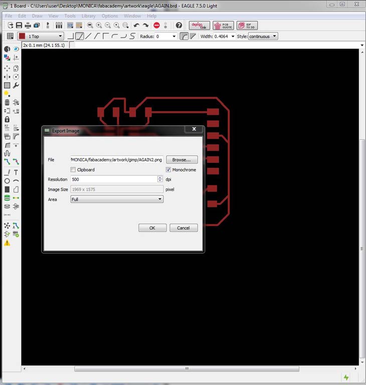
I imported these monochrome images into gimp to double check sizes, crop the canvas and invert colours for outline.
I opened and edtied the two files simultaneously as I wanted to ensure that the canvas size and placement was exactly the same to avoid having milling and cutting problems.
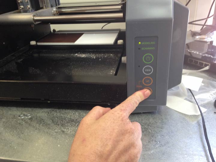
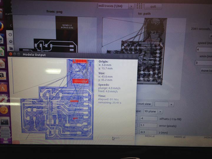
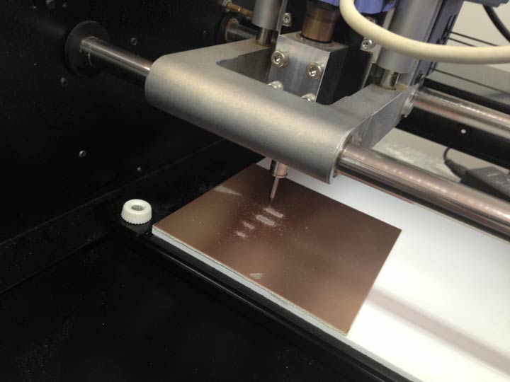
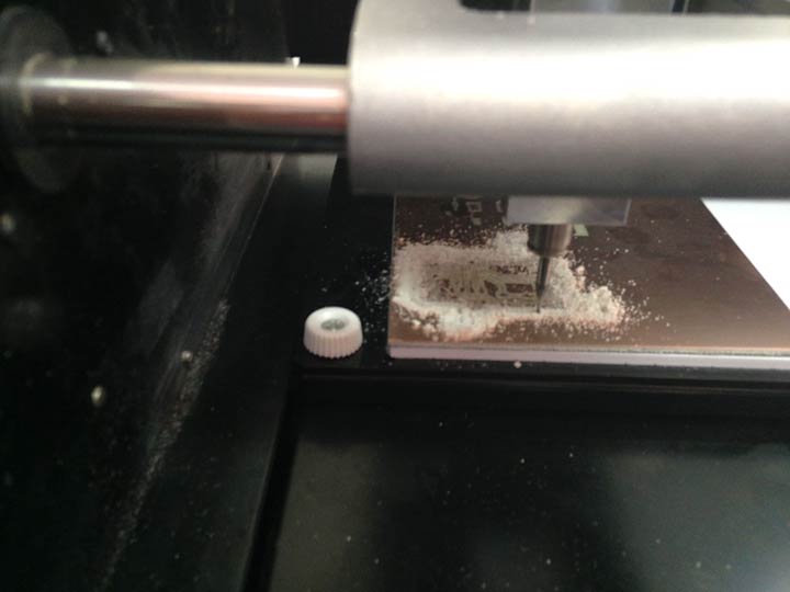
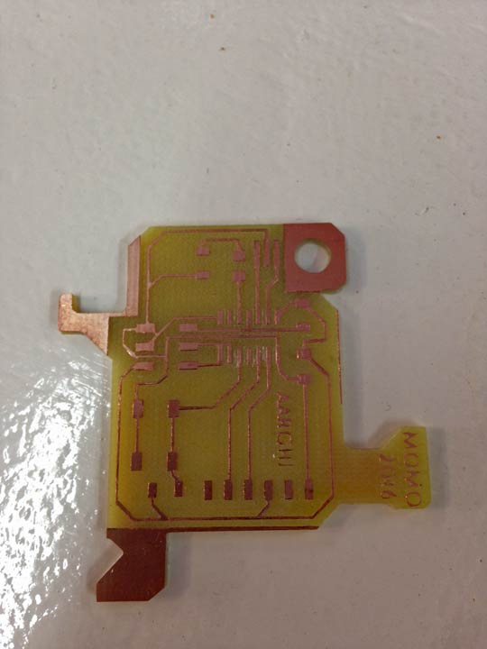
As you can see I inverted the colour on the outline file, and added text to the milling fileusing the rulersd as guides. I flattened the images and saved again as .png. This I took to the modella for milling and cutting. I set up the terminal and modeela as per FABISP week 04
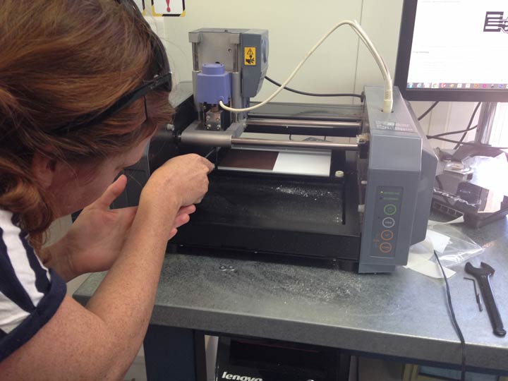
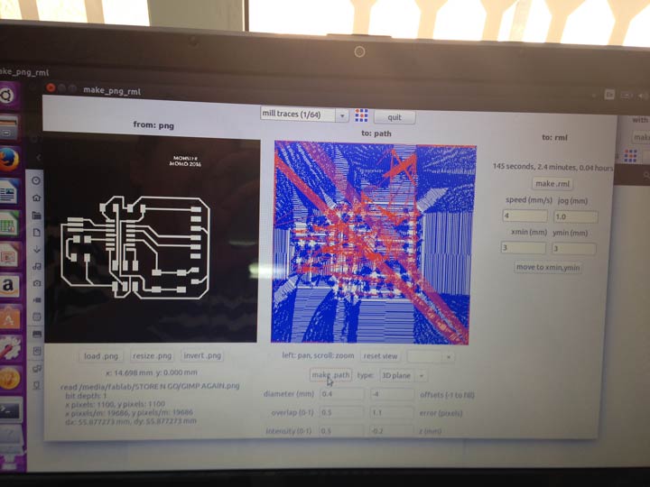
The path was very big and would take quite long to mill, so I went back to gimp and added some white space around the lines to lessen the machine time. I also made the etxt quite a lot bigger.
I also had to make the outside of the outline of my cutting file black as it would not read to make path the thin single line.
HELLO SOLDERING {UPDATE}
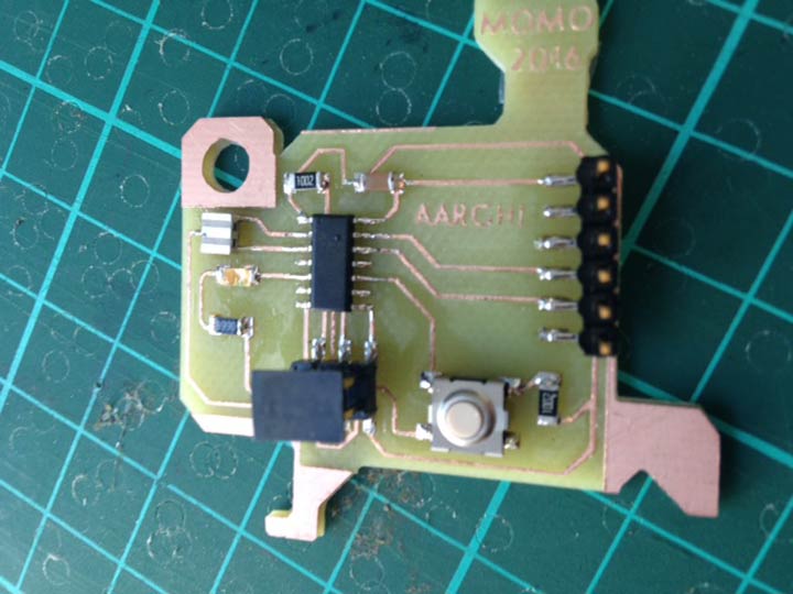
Our components have arrived!
I immediately soldered the components!
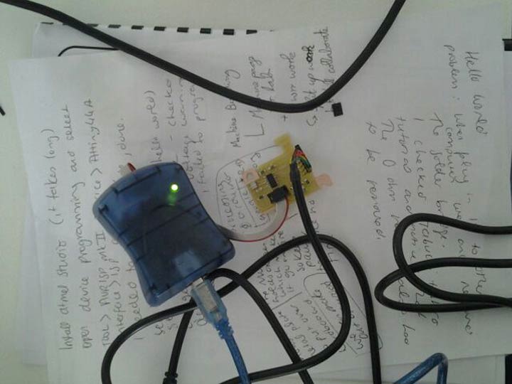
But when it came to programming, again there were problems... After many an agonising back and forth between linux and windows, installing, updating and ensuring that we had all the drivers and programmes it still would not programme the board. I did at some point get the light to blink, but it wasn't blinking as set, so not sure how that happened. I believe this may indicate a oscillation problem with the crystal, I have a suspicion that something is very wrong.
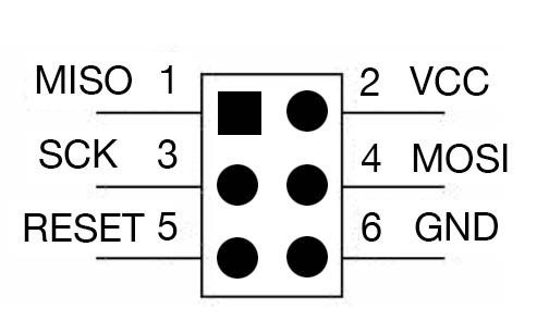
Ohad and I, went step by step through the set-up of a new windows computer, to start fresh so to say, and during this time the main problem reported using arduino IDE and AVR programmer, that the MOSI was the issue. Here is a list of errors.
I tried to desolder the FTDI connector, to check for solder bridges. I managed, gracefully, to rip up most the copper ad had to re mill and solder a new board. After this I tried to run the programme again and got the exact same MOSI error. At this point Ohad suggested that the AVR may be the cause of our problems.
Downlad my working files HERE.